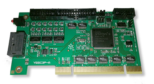
YSSC3(H)P is a PCI interface adapter compatible with Mitsubishi MR-J3/J4 SSCNET III (III/H) network servo amplifiers. It supports up to 16 connected drives in position or velocity control mode. The card also features general-purpose I/O headers for connecting to limit switches and relays. The software includes LinuxCNC 2.7 driver module and an optional patch for absolute encoder support.
SSCNET is a synchronous high-speed network for servo drives and motion controllers. SSCNET only requires a simple daisy chain wiring between servo amplifiers. See Mitsubishi documentation for details.

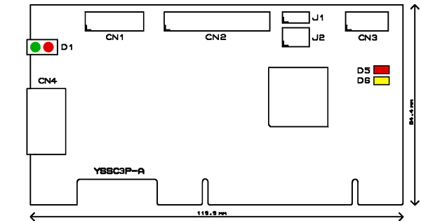
The card layout showing connectors and indication LEDs:

| J1 — CN2 power | ||
|---|---|---|
| 1-2 | CN2 pins 18, 20, 22, 24, 26 connect to GND | |
| 2-3 | --//-- to +5V* | |
| J2 — JTAG | |||
|---|---|---|---|
| 1 | TCK | 2 | GND |
| 3 | TDI | 4 | TDO |
| 5 | TMS | 6 | VCC 3.3V |
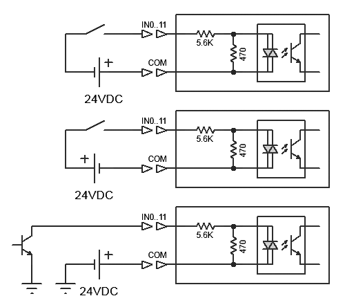
CN1 contains 12 optoisolated digital inputs. External 24VDC field power supply is required for operation. Example connection of open-collector outputs or mechanical switches is shown on schematics. Inputs can be either common anode or cathode. They are divided into 2 groups: 0-7 and 8-11
| CN1 | |||
|---|---|---|---|
| 1 | IN0 | 2 | IN1 |
| 3 | IN2 | 4 | IN3 |
| 5 | IN4 | 6 | IN5 |
| 7 | IN6 | 8 | IN7 |
| 9 | IN8 | 10 | IN9 |
| 11 | IN10 | 12 | IN11 |
| 13 | COM0-7 | 14 | COM8-11 |
Example connections:

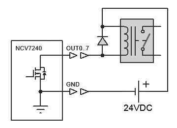
CN3 has 8 open-drain outputs from NCV7240 IC. Each output is rated to 600mA/36V max.
| CN3 | |||
|---|---|---|---|
| 1 | OUT0 | 2 | OUT1 |
| 3 | OUT2 | 4 | OUT3 |
| 5 | OUT4 | 6 | OUT5 |
| 7 | OUT6 | 8 | OUT7 |
| 9 | GND | 10 | GND |
Example connections:

CN2 connector is intended for daughter boards.
All IN12..IN28 lines are 3.3V LVTTL and are 5V tolerant.
Pins 18, 20, 22, 24, 26 optionally provide 5V power to external devices. The power is taken from the PCI bus and fused to 500mA.
| CN2 | |||
|---|---|---|---|
| 1 | IN28 | 2 | IN27 |
| 3 | IN26 | 4 | IN25 |
| 5 | IN24 | 6 | IN23 |
| 7 | IN22 | 8 | IN21 |
| 9 | IN20 | 10 | GND |
| 11 | IN19 | 12 | GND |
| 13 | IN18 | 14 | GND |
| 15 | IN17 | 16 | GND |
| 17 | IN16 | 18 | GND or +5V |
| 19 | IN15 | 20 | GND or +5V |
| 21 | IN14 | 22 | GND or +5V |
| 23 | IN13 | 24 | GND or +5V |
| 25 | IN12 | 26 | GND or +5V* |
Alternative CN2 pins functions depend on the mux configuration